- Hjemmeside /
- Bøger /
- Engineering & Transportation /
- Engineering /
- Electrical & Electronics /
- Elektronik /
- Microelectronics /
- SEMICONDUCTOR FABRICATION: A Practical Guide ...
0 ratings


Vare #:
270179661
SEMICONDUCTOR FABRICATION: A Practical Guide to Modern Chip Making, Advanced Nodes, EUV Lithography, and Yield Optimization (Huds)
Vare #:
270179661
DKK 849
Prisdetaljer
Eksklusive forsendelses- og toldgebyrer ( Forsendelses- og toldgebyrer beregnes ved checkout )
*Alle varer importeres fra US
0 ratings
Skriv en anmeldelse
På lager
 Importeret fra USA butik
QTY:
Bestil nu og få den omkring Torsdag, Oktober 29
Sikker transaktion
Ubuy arbejder hårdt for at beskytte din sikkerhed og dit privatliv. Vores avancerede betalingssikkerhedssystem sikrer fortrolighed ved at kryptere dine oplysninger under transmission ved hjælp af AES (Advanced Encryption Standards) og SSL (Secure Socket Layer) protokoller. Dine betalingsoplysninger er 100% sikre, da vi ikke deler dine betalingsoplysninger med tredjepartssælgere.
Vores bedste logistikpartnere


Hurtig
levering

Gratis
returnering*

Sikker emballering

100 % originale produkter'

PCI DSS Compliance

ISO 27001 Certified



Note: Step Down Voltage Transformer required for using electronics products of US store (110-120). Recommended power converters Køb nu.


Produktdetaljer
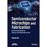
- Every layer on a modern chip is the result of a decision someone had to defend: which process, which parameter window, which trade-off to accept. This book is about making those decisions with understanding rather than habit.A recipe can be followed without being understood — until something drifts. A film comes out thin at the wafer edge. Critical dimensions widen after a resist change. A via chain fails electrical test and nobody can say which module owns the problem. Engineers and technicians who know what each step is physically doing can reason their way to the cause. Those who know only the recipe are left guessing, and the guessing is expensive.This guide builds that reasoning process by process. Each unit operation is developed from the physics and chemistry that govern it, then followed onto the factory floor: the equipment that performs it, the parameters that control it, the failure modes that limit it, and the measurements that prove it worked. Every worked example is carried through in SI units with the units tracked explicitly, so the arithmetic can be reproduced, checked and adapted to your own numbers.What you will be able to work with:▪ Die per wafer, cost per good die, and how a change in yield moves both▪ Oxide growth in the linear and parabolic regimes, and the choice between dry and wet oxidation▪ Implant dose, projected range, straggle and junction depth — and when channelling will distort a profile▪ Resolution and depth-of-focus relationships, and what a given exposure approach can realistically print▪ The selectivity, anisotropy and damage arguments behind wet, plasma and atomic-layer etching▪ Deposition selection by step coverage, thermal budget and film stress▪ Control charts, process capability indices, and the separation of random from systematic yield lossThe coverage runs the length of the flow: crystal growth and wafer preparation, contamination control, thermal oxidation, diffusion and ion implantation, photolithography including extreme-ultraviolet and high-numerical-aperture exposure, etching, thin-film deposition, chemical mechanical planarization, copper interconnect and low-permittivity dielectrics, front-end device integration, advanced nodes and chiplet packaging, metrology and defect inspection, yield and reliability engineering, and assembly, packaging and final test. 151 figures, 74 worked examples and 54 comparison tables support the text, and each of the 15 chapters opens with learning objectives and closes with a summary.It is written for students entering microelectronics, for process and equipment technicians who want the reasoning behind their recipes, and for practising engineers moving between modules. First-year chemistry and physics and elementary calculus are the only prerequisites.Add this practical resource to your bench and start working through the calculations, trade-offs and control decisions that a fab makes every day.
| Publisher | Independently published |
| Publication date | August 9, 2026 |
| Language | English |
| Print length | 374 pages |
| ISBN-13 | 979-8191781785 |
| Item Weight | 2.28 pounds (1.03 kg) |
| Dimensions | 8.49 x 1.04 x 11.24 inches (21.6 x 2.6 x 28.5 cm) |
| Book 1 of 2 | Huds |
Produktbeskrivelse
SEMICONDUCTOR FABRICATION: A Practical Guide to Modern Chip Making, Advanced Nodes, EUV Lithography, and Yield Optimization (Huds)
Har du spørgsmål? Chat med os
Kundespørgsmål og svar
-
spørgsmål:
Hvordan shopper man SEMICONDUCTOR FABRICATION: A Practical Guide to online fra Ubuy?
svar: Det er nemt at shoppe SEMICONDUCTOR FABRICATION: A Practical Guide to online fra Ubuy.. Du skal bare søge efter produktet, vælge din forsendelsesmetode, mens du tjekker ud og få det leveret til dit sted. -
spørgsmål:
Er SEMICONDUCTOR FABRICATION: A Practical Guide to tilgængelig til at handle online i Faroe Islands?
svar: Ja, hos Ubuy Faroe Islands er dette produkt tilgængeligt, så du kan handle til en rimelig pris.. SEMICONDUCTOR FABRICATION: A Practical Guide to er ikke tilgængelig lokalt, men du kan stole på os med vores ekspresforsendelsestjenester. -
spørgsmål:
Hvor lang tid tager det at få produktet efter at have afgivet ordren?
svar: Leveringstiden for dit bestilte produkt varierer alt efter, hvad du har bestilt, og den forsendelsesmetode, du har valgt.. Den estimerede leveringstid er nævnt under købsprocessen, så vær ubekymret, mens du handler.
Microelectronics Editorial Review
Ingen redaktionelle anmeldelser fundet
Kundeanmeldelser & vurderinger
1 kundebedømmelser
-
5 stjerne
100%
-
4 stjerne
0%
-
3 stjerne
0%
-
2 stjerne
0%
-
1 stjerne
0%
Anmeld dette produkt
Del dine tanker med andre kunder
Customers also viewed these products

Produktets prishistorik
Vigtig information
- Begrænsninger: For produkter, der forsendes internationalt, bemærk venligst, at eventuel producentgaranti muligvis ikke er gyldig; producentens serviceordninger er muligvis ikke tilgængelige; produktmanualer, instruktioner og sikkerhedsadvarsler er muligvis ikke på destinationslandets sprog; produkterne (og det medfølgende materiale) er muligvis ikke designet i overensstemmelse med destinationslandets standarder, specifikationer og mærkningskrav; og produkterne opfylder muligvis ikke destinationslandets krav til spænding og andre elektriske standarder (hvilket kan kræve brug af en adapter eller transformer, hvis relevant). Modtageren er ansvarlig for at sikre, at produktet lovligt kan importeres til destinationslandet. Ved bestilling hos Ubuy eller dets datterselskaber er modtageren importøren og skal overholde alle love og regler i destinationslandet.
- Det er ikke alle de produkter som vises på Ubuy som er til salg, idet Ubuy er en global søgemaskine. Produkterne er underlagt eksport-/handelsregler.
DKK 849
Bestil nu og få den omkring Torsdag, Oktober 29
Dette produkt er ikke begrænset i mit land. (Klik venligst på linket ovenfor, hvis dette produkt ikke er begrænset i dit land, så vil vores team gennemgå det og godkende det.)
QTY:
Sikker transaktion
PCI DSS-kompatibel og ISO 27001:2022-certificeret, med krypteret betaling og fuld køberbeskyttelse på hver ordre
Vores bedste logistikpartnere
Hurtigste grænseoverskridende levering
Ubuy-garanti
Oplev bekymringsfri shopping med 100 % originale produkter, PCI DSS-kompatibel betalingssikkerhed, ISO 27001-certificeret databeskyttelse, den hurtigste grænseoverskridende levering, gratis returnering* og sikker emballage på hver ordre.